What is Moore’s Law and Why is it Slowing?
Nanoscale Transistor Architectures: Gate-All-Around and Nanosheets
2D Materials and Quantum-Engineered Channels
EUV Lithography and the Challenge with Patterning
Quantum and Neuromorphic Computing
Costs, Manufacturability, and Scalability
Nanotechnology and the Future of Moore’s Law
References and Further Readings
Nanotechnology is helping extend the computing advances once driven by Moore’s Law, even as traditional silicon scaling becomes harder to sustain.
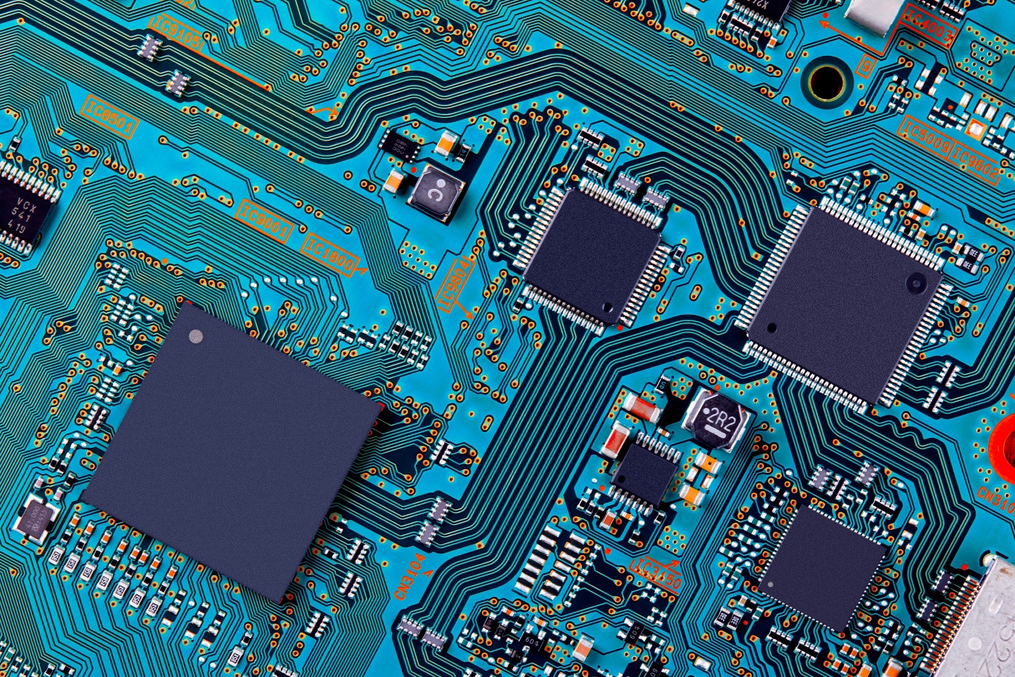 Image Credit: raigvi/Shutterstock.com
Moore’s Law helped define the digital age by linking smaller transistors to faster, cheaper, and more efficient chips. That trend is now slowing as silicon approaches physical, technical, and economic limits. In response, researchers and chipmakers are redesigning devices at the nanoscale through new transistor architectures, new materials, advanced lithography, and alternative computing models.1
What is Moore’s Law and Why is it Slowing?
Moore’s Law is not a law of physics but an empirical trend. In 1965, Gordon Moore observed that transistor density on integrated circuits was doubling roughly every two years. For decades, that pattern held. As transistors shrank, chips became faster, cheaper, and more energy efficient, supporting the rise of personal computers, smartphones, and modern digital infrastructure.1-2
That pace is now slowing for three connected reasons. First, there are physical limits. As gate lengths fall below roughly 10-20 nm, quantum tunneling and leakage currents become harder to control, while heat generation per unit area rises sharply.1-2
Second, there are material limits. Silicon begins to show constraints in carrier mobility and dielectric integrity at these dimensions, making further improvements more difficult.1-2
Third are the economic limits. Each new fabrication node demands more expensive tools and processes, including extreme ultraviolet (EUV) lithography, which has pushed development and production costs much higher.1
Nanoscale Transistor Architectures: Gate-All-Around and Nanosheets
To keep scaling performance, the semiconductor industry has moved from planar transistors to fin-field-effect transistors (FinFETs), and now toward gate-all-around (GAA) and nanosheet architectures.3
In a GAA nanosheet transistor, the channel is made from vertically stacked silicon nanosheets, each fully surrounded by the gate. This structure improves electrostatic control and reduces leakage much more effectively than earlier designs. At the nanoscale, stronger gate-channel coupling helps limit short-channel effects and improve switching behavior.3
These designs also create new challenges.
The stacked geometry and the surrounding low-conductivity dielectrics can trap heat, leading to stronger self-heating effects that reduce mobility and shift the threshold voltage. To manage this, researchers are investigating hybrid channel designs, more thermally conductive dielectrics, and multi-stacked nanosheet layouts that better balance leakage, performance, and thermal reliability.4
2D Materials and Quantum-Engineered Channels
Beyond silicon, two-dimensional materials such as transition metal dichalcogenides, including MoS2 and WS2, as well as black phosphorus, offer atomically thin channels with tunable band gaps and strong carrier transport properties. These materials can be stacked into vertical heterostructures that function as nanoscale transistors, with properties shaped by layer thickness and interlayer coupling.5-6
From a materials perspective, 2D channels are attractive because their thickness is only a few atomic layers. That helps suppress unwanted leakage and reduces some tunneling problems, while still allowing practical lateral device dimensions.5
The difficulty is integration. Large-scale CMOS manufacturing still struggles with contact resistance, interface defects, and processing constraints, especially when high throughput and low thermal budgets are required.6
Even so, solution-processable 2D inks and room-temperature printing approaches are creating plausible routes toward flexible, scalable nanoelectronics. In reality, these materials are likely to begin by complementing silicon in specialized applications before attempting complete replacement.6
EUV Lithography and the Challenge with Patterning
Keeping Moore’s Law going also depends on patterning smaller and smaller features with consistent precision. EUV lithography, with a wavelength of about 13.5 nm, enables half-pitches under 20 nm and has become essential for advanced nodes at Intel, TSMC, and Samsung.7
In practice, this means features once patterned in multiple steps with deep-ultraviolet light can now be written more directly, improving precision and reducing overlay errors. Nanotechnology also plays a central role in the lithography tools themselves. Multilayer mirrors and advanced patterning strategies are engineered at the nanoscale to reduce absorption and distortion of the EUV beam.7-8
Looking ahead, the industry is exploring high numerical aperture EUV as well as possible next-step methods such as directed self-assembly and nanoimprint lithography. The biggest challenge seems to be keeping critical dimension uniformity below the nanometer scale across the full 300 mm wafers while still controlling cost and throughput.7-8
Quantum and Neuromorphic Computing
 Image Credit: Gorodenkoff/Shutterstock.com
Some researchers are extending the idea behind Moore’s Law by changing the computing model itself, rather than relying on miniaturizing transistors.
Quantum computing uses superposition and entanglement to solve certain classes of problems in fewer steps than classical systems. Even though qubits do not follow the same density scaling pattern as transistors, they offer another path to higher functional performance.9
Neuromorphic chips take a different approach. They mimic the brain’s spiking neuron architecture and use massively parallel, low-precision operations that can outperform conventional CPUs on pattern recognition and inference tasks while using much less power.9
Both approaches depend heavily on nanoscale engineering. Memristive devices based on oxide thin films or 2D heterostructures can store and process information within a single nanoscale element, reducing the separation between memory and logic.9
Each of these avenues has value. In the long run, quantum-AI hybrids and memristor-based reservoir computing may improve useful computing performance even if traditional transistor counts stop growing at the same historic rate.9
Costs, Manufacturability, and Scalability
Nanotechnology-based solutions have evidenced promise, but as with all science, they come with trade-offs.
Complex 3D device architectures such as stacked nanosheet FETs add fabrication steps, increase defect sensitivity, and make thermal management more difficult. Those factors can reduce yield and increase capital costs.4
EUV scanners and high-NA tools are also extremely expensive. They require specialized cleanrooms, materials infrastructure, and process control, which limits how many companies can realistically compete at the leading edge.3
Other platforms, including many 2D material devices and quantum or neuromorphic systems, are still at the laboratory or early application stage. In many cases, long-term reliability, throughput, and large-scale process integration remain uncertain. Bringing silicon, oxides, 2D layers, and new interconnects into a single, contamination-free, drift-free manufacturing flow remains a major nanofabrication challenge.5
Nanotechnology and the Future of Moore’s Law
In a strict sense, Moore’s Law as a simple transistor-density-doubling trend is already decelerating and is unlikely to return to its mid-20th-century cadence. However, nanotechnology is extending the spirit of Moore’s Law by enabling new degrees of freedom.
Those gains now come from several directions at once: new materials, 3D transistor architectures, atomically thin channels, and non-classical computing systems that can deliver more performance per unit area, power, or cost.1-2
From a material-and-nanoscale-engineering perspective, the question is shifting to how industry can balance innovation with manufacturability. Gate-all-around nanosheets and EUV lithography are already in production; 2D materials and neuromorphic fabrics are likely to mature over the next decade into specialized accelerators rather than universal CPUs.2
These technologies may not preserve Moore’s Law in its original form, but they can carry forward its central promise: more capable, more efficient, and more specialized computing beyond the practical limits of classical silicon scaling.
References and Further Readings
- Wu, J., Shen, Y.-L., Reinhardt, K., Szu, H., Dong, B., A nanotechnology enhancement to Moore′ s Law. Applied Computational Intelligence and Soft Computing 2013, 2013 (1), 426962. DOI:10.1155/2013/426962, https://www.hindawi.com/journals/acisc/2013/426962/.
- Smith, B., How Does Moore's Law Relate to Nanotechnology? AZoNano 2023.
- Wang, M., A review of reliability in gate-all-around nanosheet devices. Micromachines 2024, 15 (2), 269. DOI:10.3390/mi15020269, https://www.mdpi.com/2072-666X/15/2/269.
- Li, Y. et al. Comprehensive electrothermal characterization of shrunk nanosheets in gate-all-around field-effect transistors. Micro and Nanostructures 2025, 206, 208213.
- Iannaccone, G., Bonaccorso, F., Colombo, L., Fiori, G., Quantum engineering of transistors based on 2D materials heterostructures. Nature nanotechnology 2018, 13 (3), 183-191. DOI:10.1038/s41565-017-0028-5, https://www.nature.com/articles/s41565-017-0028-5.
- Osama, M., 2D Material Transistors Make Flexible Electronics Cleaner and Cheaper. AZoNano 2025.
- EUV lithography optics from ZEISS New light for digitalization. https://www.zeiss.com/semiconductor-manufacturing-technology/inspiring-technology/euv-lithography.html.
- Levinson, H. J., Challenges and limits to patterning using extreme ultraviolet lithography. Journal of Micro/Nanopatterning, Materials, and Metrology 2025, 24 (1), 011005-011005. DOI:10.1117/1.JMM.24.1.011005, https://www.spiedigitallibrary.org/journals/journal-of-micro-nanopatterning-materials-and-metrology/volume-24/issue-1/011005/Challenges-and-limits-to-patterning-using-extreme-ultraviolet-lithography/10.1117/1.JMM.24.1.011005.full.
- Mehonic, A. et al. Roadmap to neuromorphic computing with emerging technologies. APL Materials 2024, 12 (10).
Disclaimer: The views expressed here are those of the author expressed in their private capacity and do not necessarily represent the views of AZoM.com Limited T/A AZoNetwork the owner and operator of this website. This disclaimer forms part of the Terms and conditions of use of this website.