Feb 25 2009
Scientists and engineers the world over have thought for years that the next generation of smaller, more-efficient electronic and photonic devices could be based on the use of carbon nanotubes, structures 10,000 times thinner than a human hair but with tremendous potential.
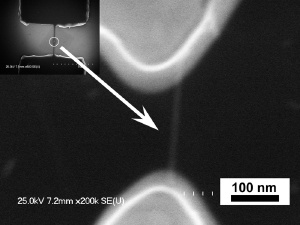 This is a black-and-white image of a micrograph from a scanning electron microscope of the electrodes (inset) and the single-walled carbon nanotube bridge structure. A colorized version of the micrograph of the electrodes was the cover photo for the Jan. 14 issue of Nanotechnology.
Laboratories are able to create millions of the structures using a process called chemical vapor deposition. The problem has always been finding a way to manipulate something that small so they'll line up in a way that might be useful.
Now, however, a discovery by a team of researchers at the University of Nebraska-Lincoln, led by professor Yongfeng Lu and postdoctoral researcher Yunshen Zhou, may provide a pathway to a solution, and with little or no manipulation necessary.
Using a process based on optical near-field effects, Lu and his team in UNL's Laser Assisted Nano-Engineering Lab created nanoscale devices based on connecting sharp-tipped electrodes with individually self-aligned carbon nanotubes.
Previous efforts in this area by other research groups tried to use advanced instrumentation to manipulate carbon nanotubes after growth. But Lu said that approach is only good for research purposes because it's time consuming and expensive.
"With our method, there's no requirement for expensive instrumentation and no requirement for tedious processes. It's a one-step process," he said. "We call it 'self-aligning growth.' The carbon nanotubes 'know' where to start growth.
"In previous efforts, they could only manipulate carbon nanotubes one piece at a time, so they had to align the carbon nanotubes one by one. For our approach using optical near-field effects, all locations with sharp tips can accommodate carbon nanotube growth. That means we can make multiple carbon nanotubes at a time and all of them will be self-aligned."
Nevertheless, the UNL team has not yet been able to produce large numbers self-aligned carbon nanotubes, but Lu said he and his team see potential for significant expansion that could lead to new applications in devices such as biosensors, light emitters, photon sensors, tiny molecular motors and memory cells.
"We have shown that we can use optical near-field effects to control growth for a small amount of carbon nanotubes," said Lu, Lott professor of electrical engineering at UNL. "We want to make this process scalable so it can be used to make large numbers at a time so we can make a circuit or a system by this approach."
The research was the cover story for the Jan. 14 issue of Nanotechnology, a leading international journal published by the Institute of Physics in the United Kingdom. The research was supported by a grant from the National Science Foundation. Initial funding was provided by the Nebraska Research Initiative.