Feb 5 2010
Scientists of the research group of Prof. Dr. Alfred Meixner and Dr. Dai Zhang from the Institute of Physical and Theoretical Chemistry at the University of Tübingen have developed a near-field microscope that can measure the optical properties of e. g. semiconductor thin films with a spatial resolution and sensitivity long thought unachievable due to fundamental physical laws (diffraction limit).
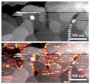 The upper panel shows the topographical measurement of a diindenoperylene film. Lighter shades stand for higher areas, darker ones for lower areas. In the lower panel the topographical and the optical measurements are superimposed – the latter one in the red and yellow colour range; the brighter the colour, the higher the luminescence intensity. Copyright: Research Group of Prof. Meixner, University of Tübingen
Both the optical spectrum and the topography of a surface can be mapped simultaneously with nanometre precision – a nanometre corresponding to one millionth of a millimetre. “Molecular steps of a semiconductor film appear as distinct bright stripes of approximately 17 nanometres width. We obtained new insights that cannot be obtained with any other method,” says Alfred Meixner. The findings are published on the 5th of February 2010 in the journal Physical Review Letters. The results were obtained in collaboration with Ute Heinemeyer and Prof. Dr. Frank Schreiber (Institute of Applied Physics, University of Tübingen) and with Dr. Reinhard Scholz (Technical University of Munich).
Semiconductors made of organic thin films play an important role in new electronic applications, e.g. in organic solar cells, where solar power is converted to electric current, or in organic light emitting diodes (OLEDs) for flexible high resolution displays. The electronic and optical properties of these films differ greatly from the properties of the single organic molecules of which they consist. Especially the microscopic structure is not yet well understood, though molecular islands, edges and defects strongly influence the average film properties.
These microscopic structures were now optically detected by the near-field microscope in Tübingen. Thereto, an extremely fine gold tip is approached closely (one to three nanometres) to the semiconductor surface, where it is additionally illuminated by a tightly focused laser beam. “We obtained nanometre resolution and an optical luminescence enhancement of up to one million,” explains Alfred Meixner. “This high enhancement factor is possible because the tip is in the focus of a parabolic mirror: This combination yields a perfect optical antenna. The gold tip concentrates the light locally into the nanometre sized gap between the tip apex and the sample surface and thereby generates an optical near field which in turn excites the sample. Vice versa, photons that are generated by the sample inside the near-field area are collected by the tip and the parabolic mirror and directed onto a sensitive detector.”
The near-field measurements of the semiconductors made of diindenoperylene (DIP) molecules revealed that the edges of the DIP nano terraces radiate stronger than the bulk. These edges are one to three molecular layers high and appear as bright stripes of approximately 17 nanometres. This is due to electron hole pairs in the semiconductor DIP, so called excitons, which are induced as well as detected by the near field of the tip. “If our tip was not there, the excitons would mainly decay thermally”, explains Alfred Meixner. “This breakthrough could lead to the near-field microscopy becoming a valuable method for materials research,” Reinhard Scholz and Frank Schreiber agree.