Feb 20 2019
Ever since graphene was discovered, researchers have tried to exploit the material to create nano-sized electronics. However, since graphene is just an atom thick, all atoms are exposed to the atmosphere, and even small amounts of flaws and impurities hinder its properties. Currently, Graphene Flagship researchers at DTU, Denmark resolved this issue by shielding graphene with insulating layers of hexagonal boron nitride, another two-dimensional (2D) material possessing insulating properties.
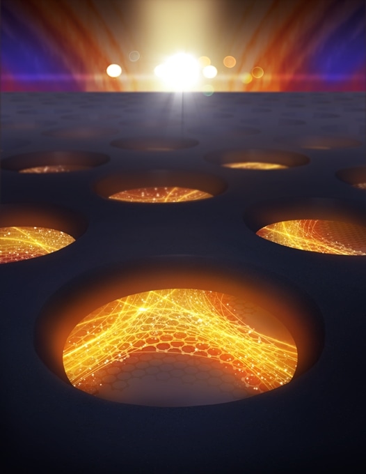 Graphene Flagship researchers solved one of the challenges of making graphene nano-electronics effective: to carve out graphene to nanoscale dimensions without ruining its electrical properties. This allowed them to achieve electrical currents orders of magnitude higher than previously achieved for similar structures. The work shows that the quantum transport properties needed for future electronics can survive scaling down to nanometric dimensions. (Image credit: Carl Otto Moesgaard)
Peter Bøggild, scientist at Graphene Flagship partner DTU and coauthor of the paper, explains that even though “graphene is a fantastic material that could play a crucial role in making new nano-sized electronics, it is still extremely difficult to control its electrical properties.” Since 2010, researchers at DTU have attempted to modify the electrical properties of graphene, by making an extremely fine pattern of holes, thereby creating channels through which electric power can flow easily. “Creating nanostructured graphene turned out to be amazingly difficult, since even small errors wash out all the properties we designed it to have,” states Bøggild.
At present, scientists from Graphene Flagship partner DTU have made huge progress. Bjarke Jessen and Lene Gammelgaard encapsulated graphene with another 2D material, hexagonal boron nitride, which is quite similar to graphene, but electrically insulating. Then, using nanolithography, they cautiously drilled nanoscopic holes in graphene via the protective layer of boron nitride. The diameter of the holes is approximately 20 nm, and the holes are separated from each other at 12 nm distance. This extraordinary precision facilitates the transmission of electrical current via the graphene which is 100-1000 times more than usual numbers for lithographically carved nanographene.
“When you make patterns in a material like graphene, you do so in order to change its properties. However, what we have seen throughout the years is that when we shape graphene on this fine scale, it does not behave like graphene anymore—there is too much disorder,” explains Bøggild. “Many scientists have abandoned nanolithography in graphene on this scale, but now we have figured out how it can be done—you could say that the curse is lifted,” he adds.
We have shown that we can control graphene’s band structure and that deterministic design of nanoelectronics is realistic. Looking solely at electronics, this means that we can make insulators, transistors, conductors and perhaps even superconductors, as our nanolithography can preserve the subtle inter-layer physics that was recently shown to lead to superconductivity in double-layer graphene. However, it goes way beyond that. When we control the band structure, we have access to all of graphene’s properties. In other words, we could sit in front of the computer and dream up other applications—and then go to the laboratory and make them happen. Here are plenty of practical challenges, but the fact that we can tailor electronic properties of graphene is a big step towards creating new electronics with extremely small dimensions.
Peter Bøggild, Study Co-Author and Scientist, DTU, Graphene Flagship.
Controlling the electronic properties of graphene by nano-pattering offers an additional degree of freedom for the design of electronic and photonic devices, which was so far not accessible. The researchers from Graphene Flagship partner DTU and their co-workers now discovered a unique way for nano-patterning of graphene without seeing the limitations of patterning introduced defects. This was the key enabling step for using the nano-patterning induced electronic properties of graphene in real device and we are expecting significant advances especially for nano-electronics and photonics based on these results.
Daniel Neumaier, Division Leader for Electronics and Photonics Integration, Graphene Flagship.
Andrea C. Ferrari, Science and Technology Officer of the Graphene Flagship and Chair of its Management Panel added how “patterning of graphene to create nano-electronic devices was one of the first approaches attempted to exploit this unique material into devices. However, after an initial flurry of publications, the amount of damage produced was so much that this line of research was almost entirely abandoned. The work presented here shows how the long term nature of the Flagship allows scientists to pursue and solve even apparently intractable problems. This will rejuvenate the interest in graphene nanoelectronics, and could lead to a variety of useful devices, previously hampered by defects.”