The material gallium nitride (GaN) is extensively used in optoelectronic devices such as Light Emitting Diodes (LEDs). LED structures are typically grown by epitaxy on sapphire substrates, but due to cost reasons silicon emerges as a potential competitor. Yet, the vast misfit and the difference in coefficient of thermal expansion that exists between the nitrides and silicon result in numerous dislocations and possible cracks, which often appear during the cooling stage in the growth process. As both dislocations and cracks are damaging for LED applications, it is essential to establish local defect concentration and other features like strain and doping.
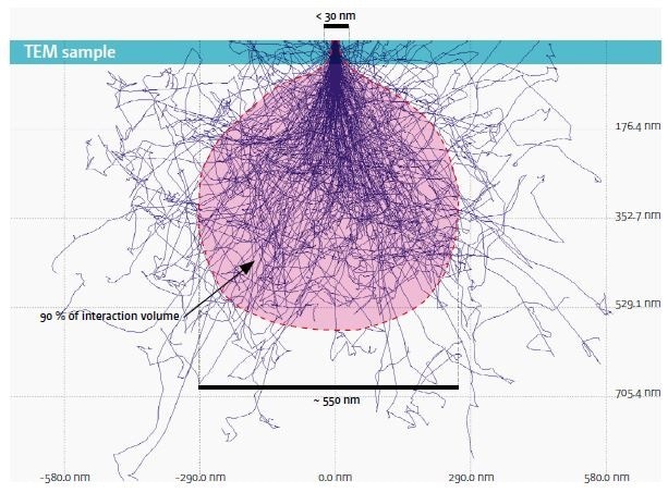
Simulation (CASINO) of the interaction volume for Ubeam=100 keV into GaN material. Using a TEM sample (width=50 nm) decreases the lateral dimensions of interaction volume from 550 nm to less than 30 nm.
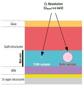
Top down view of the studied sample. Spots represent the CL resolution for TEM and bulk sample.
Cathodoluminescence (CL) Technique
The cathodoluminescence (CL) technique presents a rapid and highly relevant method for investigating GaN properties. One can directly visualize the distribution of non-radiative defects such as dislocations. The energy of below band gap emission lines enables the identification of point defects. Relevant information on the spatial variation of doping, strain, carrier concentration, and growth direction are provided by CL hyperspectral maps. In fact, the spatial resolution in CL can be greatly enhanced by limiting the size of the interaction volume between the sample and the electron beam. Thin objects such as TEM samples may be used to overcome this physical limitation. This considerably decreases the lateral size of the interaction volume from 550 nm (at a beam energy of 10 keV into GaN) to less than 30 nm.
A specific cryogenic sample holder, which is compatible with TEM samples, has been designed to carry out measurements on the Attolight CL microscope at low temperature (down to liquid He). However, the small probed volume in the sample is capable of significantly reducing the collected signal and thus limiting the measurement resolution. This complication is easily resolved by the optimized light collection of the Attolight CL system, which helps perform highly resolved hyperspectral mapping (with a very high signal-to-noise ratio) within a short period of time on cross-sectional TEM samples. Such measurements are not restricted to GaN and can be extended to other light emitting materials.
TEM sample
The protocol, depending on the Attolight CL microscope, allows for:
- Good visualization of dislocation network and correlation with TEM images obtained on the same area of the sample
- Spatial luminescence mapping of the different constituents of the stack (AlN, GaNs, quantum wells, etc)
- Estimation of the local strain and doping in the region of interfaces and dislocations through the energy shift in CL spectra
- Identification and spatial distribution of point defects
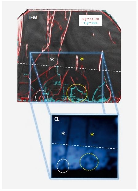
Dislocations network observed with TEM and CL on the same area of the sample.
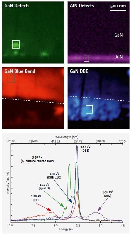
Hyperspectral mapping of the sample luminescence and related spectra.

This information has been sourced, reviewed and adapted from materials provided by Attolight.
For more information on this source, please visit Attolight.