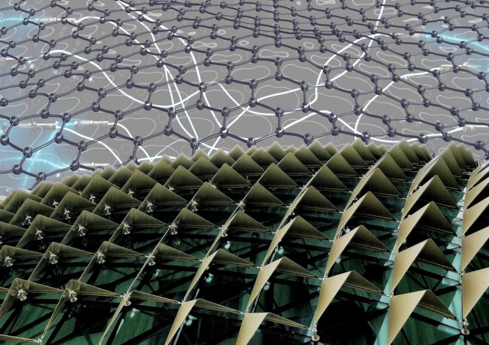
The multitude of unprecedented and useful properties of graphene have applications that span across construction, telecommunications, aerospace, energy, sensing, and many other industries. Because of the 2D geometry of graphene, the electrical, optical, chemical and mechanical properties of the material can easily be tuned by modifying the environment, because each atom in the graphene lattice is in contact with the environment on both sides of the sheet.
Very often, especially in electronic, optical, telecommunication and sensing applications, graphene is transferred on top of a SiO2 substrate. A prime example of a typical graphene structure on SiO2 is the graphene field effect transistor – GFET, a sheet of graphene connected to metal terminals on the planar substrate. The current common understanding is that graphene interacts with SiO2 through weak, long-range van der Waals forces, even though experimental evidence suggests a surprisingly strong interaction between graphene and SiO2 that affects all properties of the device.
Now, a multinational research team from Italy, Spain, Greece, and the UK has experimentally shown that surface charges on the oxide are a main factor of strong interaction between graphene and SiO2, paving the way for designing 2D material interaction with a substrate through manipulation of surface charges. Such control of graphene-substrate interactions will facilitate the development of new graphene-based microelectronic devices.
Employing several experimental methods, namely Raman spectroscopy, Scanning Kelvin Probe Microscopy, and X-ray Photoelectron Spectroscopy, the scientists studied graphene deposited on different types of silica surfaces, revealing that each of those substrates interacted with graphene in proportion to the amount of surface charge, indicating an electrostatic interaction. Raman analyses showed a shift in the characteristic spectral peaks in graphene on different substrates, whereas the other two methods clearly demonstrate different surface charge concentrations and valence band bending (due to electrostatic doping) across the different samples.
The revealed mechanism could open new frontiers in microelectronics and can be exploited in novel multifunctional devices that provide strong adhesion only at select areas. The results were published in the journal Carbon.