A new study shows that aggressively scaled 2D semiconductor nanoribbons can deliver higher current, sharper switching, and lower contact resistance, challenging the assumption that ultra-narrow channels must sacrifice performance.
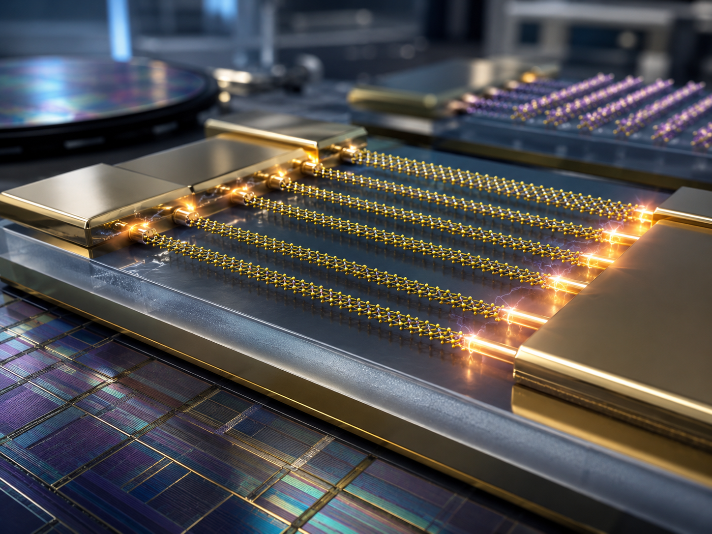
Paper: Scaling two-dimensional semiconductor nanoribbons for high-performance electronics. Image Credit: AI-generated image / OpenAI
In a recent research article published in the journal Nature Communications, researchers demonstrate that scaling the channel width of monolayer transition-metal dichalcogenide nanoribbon transistors to ~30-40 nm, within the tested range, not only preserves but also enhances device performance, achieving significantly higher on-current densities and improved electrostatics for future ultra-scaled electronics.
2D Nanoribbon Scaling Challenges
The continuous scaling of silicon transistors has driven modern electronics for decades, but as dimensions approach the nanometer regime, traditional planar architectures face fundamental physical limits. To sustain Moore’s law and enhance device density and performance, three-dimensional transistor architectures such as gate-all-around (GAA) nanoribbons and complementary field-effect transistors (CFETs) have emerged as promising solutions.
Critically, these architectures require channel widths scaling down to tens of nanometers to optimize device footprint and electrostatic control. Monolayer transition-metal dichalcogenides (TMDs), a class of atomically thin two-dimensional (2D) semiconductors, possess naturally passivated surfaces and ultrathin bodies, which are beneficial for ultimate scaling, making them prime candidates for these applications.
However, prior research mostly focused on relatively wide TMD channels (micrometer-scale widths), leaving their behavior under aggressive width scaling largely unexplored.
Nanoribbon Fabrication & Characterization
This study investigates the effect of aggressive channel-width scaling in monolayer TMD nanoribbon field-effect transistors (FETs), focusing primarily on MoS2 as a model system and extending the findings to n-type WS2 and p-type WSe2 devices. The authors fabricated nanoribbons with widths down to approximately 35 nm and channel lengths ranging from 55 nm to 75 nm.
Fabrication began with 2-inch molecular-beam epitaxy-grown monolayer MoS2 and WS2 films and 2-inch chemical-vapor-deposition-grown monolayer MoS2 and WSe2 films, which were transferred onto local bottom-gate substrates. Nanoribbons were patterned through a Cl2/O2 plasma etching process optimized to yield smooth, narrow features without compromising structural integrity. Electron-beam lithography defined both nanoribbon width and source/drain contacts, which consisted of Ni contacts to enable carrier injection, although contact-related variability remained an important consideration.
The devices incorporated ultrathin, atomic-layer-deposition-grown HfO2 dielectrics (3 nm at low temperature for MoS2 and 6 nm at higher temperature for WS2 and WSe2) on local bottom gates to ensure strong electrostatics and gate control. Scanning electron microscopy (SEM) and atomic force microscopy (AFM) verified the nanoribbon dimensions and uniformity.
Raman spectroscopy and photoluminescence (PL) mapping provided analysis of crystallinity and edge-related optical properties. Electrical characterization under vacuum conditions utilized a semiconductor parameter analyzer to measure transfer and output characteristics, enabling the extraction of figures of merit such as on-current density, subthreshold swing (SS), threshold voltage, contact resistance, and effective mobility.
Transfer length method (TLM) structures allowed quantitative contact resistance determination. Computer-aided design (TCAD) simulations, complementing experimental results, mapped the electrostatic environment and carrier distributions in scaled nanoribbons.
Performance Enhancement Mechanisms
This study demonstrates that aggressive width scaling of monolayer MoS2 nanoribbon field-effect transistors (FETs) markedly improves device performance rather than degrading it within the experimentally accessible regime. Devices with channel widths scaled from approximately 540 nm down to ~35 nm exhibit a median increase of about 42% in on-current density and a 16% reduction in subthreshold swing.
The best-performing MoS2 nanoribbon device achieves an exceptional maximum current density close to 995 μA μm-¹ at a drain-to-source voltage of 1 V and an overdrive voltage of 2.5 V, surpassing many previous monolayer TMD devices with similar channel dimensions.
Structural and optical characterizations, including Raman spectroscopy and photoluminescence mapping, confirm the preservation of crystallinity and optical quality after nanoribbon patterning, indicating minimal edge-induced disorder.
This is hypothesized to be partly related to oxygen incorporation during etching, which could passivate sulfur vacancy-related mid-gap states. TCAD simulations further reveal intensified electric fields and elevated carrier densities localized at the ribbon edges under gate bias, enhancing electrostatic channel control.
Crucially, a major contributor to performance enhancement, particularly in short-channel, contact-limited devices, is the substantial reduction in contact resistance, from ~860 Ω·μm in wider channels to approximately 270 Ω·μm in narrow nanoribbons.
This arises from more efficient side-contact injection enabled by the larger relative contribution of nanoribbon edges to contact injection and improved gate field penetration near contacts, confirmed quantitatively via TLM measurements. Although effective carrier mobility decreases moderately (~24%), likely due to edge roughness scattering and residual trap states, the overall device metrics benefit markedly from nanoribbon scaling.
Extending this platform, the authors demonstrate complementary high-performance nanoribbon FETs based on p-type WSe2 and n-type WS2 with optimized gate dielectrics. Despite WSe2 nanoribbons being wider (~80 nm) to improve fabrication yield, the NO-doped WSe2 p-FETs exhibit steep switching and a high on-current (~357 μA μm-¹), underscoring the broader versatility of the nanoribbon platform for monolayer transition-metal dichalcogenide electronics.
Implications for Future Electronics
This research presents a systematic demonstration that aggressively scaling the channel width of monolayer TMD nanoribbon transistors to as narrow as ~30-40 nm not only preserves but enhances device performance metrics relevant to nanoelectronic applications.
Achieving sub-10 nm nanoribbons with smooth edges and effective passivation will be crucial for future ultra-scaled electronics, as edge roughness and disorder-related scattering may become more significant at these dimensions and potentially offset the benefits observed at ~35 nm. Overall, this work establishes channel width as a critical nanoscale design parameter, unlocking new pathways for two-dimensional semiconductor nanoribbons to enable next-generation high-performance electronic devices in three-dimensional transistor architectures.
Download your PDF copy by clicking here.