Jul 15 2008
IMEC reports functional 0.186µm2 32nm SRAM cells made with FinFETs from which the contact layer was successfully printed using ASML's full field extreme ultraviolet (EUV) Alpha Demo Tool (ADT). Applied Materials, using its most advanced deposition systems, was key to fabricating the ultra-small circuit structures. IMEC also completed the integration and site acceptance test of the EUV ADT in its 300mm clean room. Stimulated by these milestones and with a concerted effort from all those involved in EUV research, IMEC is committed to rapidly advancing EUV for the 22nm node.
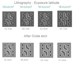 32nm SRAM device after EUV ADT exposures with various doses and after oxide etch.
To accelerate the learning on EUV patterning, IMEC decided to integrate the EUV contact photo in its 32nm SRAM vehicle. Using EUV lithography, a direct patterning approach of contact holes is proven to be feasible for integration in a 32nm technology. And the significant extendibility of EUV lithography shows promise to replace 193nm lithography for the 22nm node and beyond.
For the front-end-of-line process, IMEC used its high-k/metal-gate FinFET platform, capable of delivering SRAM cells with sizes below 0.1µm² suitable for the 22nm node. The FinFETs consist of HfO2 as dielectric and TiN as metal gate and NiPt silicide for the source/drain. The critical FinFET layers were printed using ASML’s 1700i and 1900i immersion lithography tools. The metallization of the 50nm contact holes was realized using Applied Materials most advanced contact processing modules for inter layer barrier Ti and TiN, tungsten fill and chemical mechanical polishing. .
IMEC also successfully completed the integration and site acceptance tests of the EUV ADT in its 300mm research facility. This paves the way for IMEC and its partners to fully deploy the tool and examine solutions for the 22nm node. The EUV ADT will be used in IMEC’s industrial affiliation program to identify the key critical issues for EUV lithography and to propose solutions. This research will include (1) testing and benchmarking EUV resists using the full-field exposure tool; (2) integrating EUV lithography in a full CMOS process focusing on the 22nm technology node; (3) evaluating and improving the worldwide efforts on mask technology and (4) assessing the performance and stability of the EUV ADT. .
IMEC’s core partners are being offered the opportunity to use the ADT for dedicated exposures, bringing in their own proprietary wafers and EUV reticles. .
"Although several critical issues still need to be solved, the acceptance of the ADT and successful fabrication of 32nm SRAM using EUV are important milestones in the development of EUV technology, which is considered the technology for the 22nm half pitch insertion;"said Luc Van den hove, Chief Operating Officer at IMEC. "Key to the success of our research is the presence of leading tool suppliers with their latest tools on-site, collaborative research between local staff and on-site residents from IDMs, foundries, equipment and material suppliers. Such collaborations are indispensable for the semiconductor industry to keep Moore’s momentum." .
These results were obtained in collaboration with IMEC’s sub-32nm CMOS partners including Intel, Micron, Panasonic, Qimonda, Samsung, TSMC, NXP, Elpida, Hynix, Powerchip, Infineon, TI, ST Microelectronics.