Dec 24 2014
When it comes to engineering single-layer atomic structures, "minding the gap" will help researchers create artificial electronic materials one atomic layer at a time, according to a team of materials scientists.
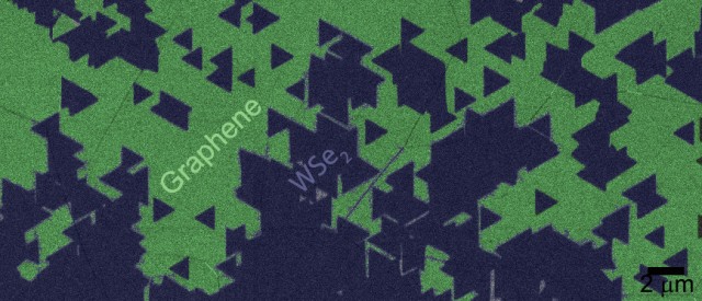
 Colorized TEM image of tungsten disulfide triangles (black) growing on graphene substrate (green). Image: UT Dallas/Penn State
The gap is a miniscule vacuum that researchers in Penn State's Center for 2-Dimensional and Layered Materials believe is an energy barrier keeping electrons from easily crossing from one layer of material to the next.
"We're still trying to understand how electrons move vertically through these layered materials, and we thought it should take a lot less energy," said Joshua Robinson, assistant professor of materials science and engineering and associate director of the 2DLM Center. "Thanks to a combination of theory and experiment, we now know we have to account for this gap when we design new materials."
For the first time, the Penn State researchers grew a single atomic layer of tungsten diselenide on a one- atom-thick substrate of graphene with pristine interfaces between the two layers. When they tried to put a voltage from the top tungsten diselenide layer down to the graphene layer, they encountered a surprising amount of resistance. About half of the resistance was caused by the gap, which introduced a large barrier, about 1 electron volt, to the electrons trying to move between layers. This energy barrier could prove useful in designing next generation electronic devices, such as vertical tunneling field effect transistors, said Robinson.
The interest in this type of material arose with the discovery of methods to make single layer graphite. The Penn State researchers use a more scalable method than early graphene makers -- chemical vapor deposition -- to deposit a single layer of crystalline tungsten diselenide on top of a few layers of graphene grown from silicon carbide.
Although graphene research exploded in the last decade, many similar solids exist that can combine to create entirely new artificial materials with unimaginable properties.
The researchers discovered that the tungsten diselenide layer grew in perfectly aligned triangular islands 1 to 3 microns in size that slowly coalesced into a single crystal up to 1 centimeter square. They reported their results in Nano Letters.
Robinson believes it will be possible to grow these crystals to industrially useful wafer-scale sizes, although it will require a larger furnace than he currently has in his lab.
"One of the really interesting things about this gap," Robinson said, "is that it allows us to grow aligned layers despite the fact that the atoms in the graphene are not lined up with the atoms in the tungsten diselenide. In fact there is a 23 percent lattice mismatch, which is huge."