Two-dimensional sheets of graphene in the form of ribbons a few tens of nanometers across have unique properties that are highly interesting for use in future electronics. Researchers have now for the first time fully characterized nanoribbons grown in both the two possible configurations on the same wafer with a clear route towards upscaling the production.
Graphene in the form of nanoribbons show so called ballistic transport, which means that the material does not heat up when a current flow through it. This opens up an interesting path towards high speed, low power nanoelectronics. The nanoribbon form may also let graphene behave more like a semiconductor, which is the type of material found in transistors and diodes. The properties of graphene nanoribbons are closely related to the precise structure of the edges of the ribbon. Also, the symmetry of the graphene structure lets the edges take two different configurations, so called zigzag and armchair, depending on the direction of the long respective short edge of the ribbon.
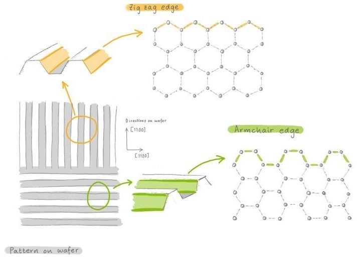
The nanoribbons were grown in two directions along ridges on the substrate. This way both the zigzag- and armchair-edge varieties form and can be studied at the same time. The positions of the atoms in the graphene layer as well as the zig zag edge can be seen from the scanning tunneling microscopy image (Å stands for Ångström, 0.1 nanometers).
The nanoribbons were grown on a template made of silicon carbide under well controlled conditions and thoroughly characterised by a research team from MAX IV Laboratory, Technische Universität Chemnitz, Leibniz Universität Hannover, and Linköping University. The template has ridges running in two different crystallographic directions to let both the armchair and zig-zag varieties of graphene nanoribbons form. The result is a predictable growth of high-quality graphene nanoribbons which have a homogeneity over a millimeter scale and a well-controlled edge structure.
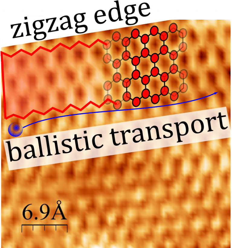
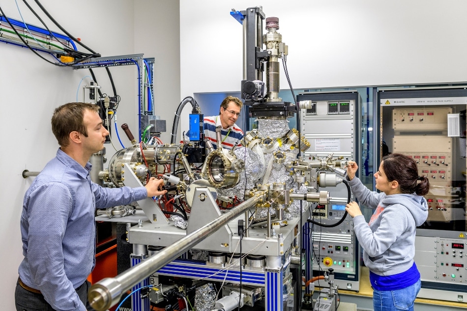
One of the new findings is that the researchers were able to show ballistic transport in the bulk of the nanoribbon. This was possible due to extremely challenging four probe experiments performed at a length scale below 100 nm by the group in Chemnitz, says Alexei Zakharov, one of the authors.
The electrical characterization also shows that the resistance is many times higher in the so called armchair configuration of the ribbon, as opposed to the lower resistance zig-zag form obtained. This hints to a possible band gap opening in the armchair nanoribbons, making them semiconducting. The process used for preparing the template for nanoribbon growth is readily scalable. This means that it would work well for development into the large-scale production of graphene nanoribbons needed to make them a good candidate for a future material in the electronics industry.
So far, we have been looking at nanoribbons which are 30–40 nanometers wide. It’s challenging to make nanoribbons that are 10 nanometers or less, but they would have very interesting electrical properties, and there´s a plan to do that. Then we will also study them at the MAXPEEM beamline, says Zakharov.
The measurements performed at the MAXPEEM beamline was done with a technique not requiring X-rays. The beamline will go into its commissioning phase this spring and will start welcoming users this year.