May 30 2008
El-Mul Technologies announced that it has gained critical knowledge that will allow commercial manufacture of its proprietary E-Beam On-a-Chip™ carbon nanotube (CNT) based field emission device.
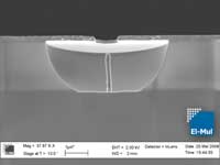 Cross-section of El-Mul's fine beam CNT field emission device, now in testing stages
Details of the achievement will be presented on June 3 at the 2008 Conference of the Nanoscience and Technology Institute (NSTI) to be held in Boston, by Mr. Sagi Daren, El-Mul’s Nano Electron Source (NES) project manager.
“Today we are offering a working industrial process to manufacture complex CNT-based electron sources with outstanding performance for real life applications,” Dr. Armin Schon, CEO of El-Mul Technologies, announced. “We can now custom design and produce sources for various applications and we will expand our offerings in the near future, both in our home markets and elsewhere.”
The company is focusing on design and manufacture of E-beam sources in two areas: well-characterized fine beam applications based on single CNT emitters, and high-current broad beam applications based on multi-beam CNT emitter arrays. Marketed as the E-Beam On-a-Chip™ platform, El-Mul’s first product is currently undergoing testing with a European partner.
Schon noted that early stages of El-Mul’s CNT electron source project were greeted with skepticism. “I heard many critical comments about the technological difficulties of such an endeavor. Today we can show that we have overcome the biggest challenge of all – high yield manufacturing.” Schon also praised the project team members. “We’ve been successful because we’ve harnessed the best properties of Israel’s high tech culture: highly qualified and motivated team members with very high tolerance for risk and disappointment, working alongside management that has the long-term vision to guide a very challenging process through to its resolution.”
El-Mul’s initial electron source device is targeted primarily for next generation scanning electron microscope (SEM) and transmission electron microscope (TEM) systems. The new device is expected to result in 30 percent higher resolution, a four-fold increase in scanning speeds, and a significant cost reduction in both manufacturing and maintenance of SEM and TEM systems.
El-Mul’s patented approach creates a MEMS-based electron source that results in superior beam brightness, narrower energy spread and smaller source size than conventional electron emitter devices. To manufacture the new device, El-Mul has also developed a proprietary chemical vapor deposition (CVD) process that grows single CNT emitters inside cathode wells 4 microns deep.
Among potential application markets for the E-Beam On-a-Chip™ platform are: sub 40 nm E-beam lithography, metrology and inspection tools (for semiconductor manufacturing); X-ray and mass spectrometry tools (for medical and life sciences); and field emission displays.
CNT-based electron source device R&D has been funded through strategic partnerships and by the Office of the Chief Scientist in Israel’s Ministry of Industry and Trade. El-Mul holds US and international patents for its R&D in this area.