eWARP is the first EBSD detector to operate via direct electron detection. Built around a Bruker-designed sensor that combines direct detection with CMOS technology, eWARP delivers exceptional performance and takes EBSD capabilities to the next level.
As the fastest and most signal-efficient EBSD detector available, eWARP can capture EBSD maps at speeds of up to 14,400 patterns per second - all while operating under low-to-medium electron beam conditions, such as an accelerating voltage of 10 kV and a probe current of 12 nA.
This unprecedented signal efficiency comes from eWARP’s wide-area pixels, which ensure a high collection rate, and its silicon sensor, optimized for the electron energies typical for electron microscope analysis, resulting in a high conversion rate.
eWARP forms the powerful core of Bruker's QUANTAX EBSD system for EBSD analysis, setting a new benchmark for speed, efficiency and ease of use.
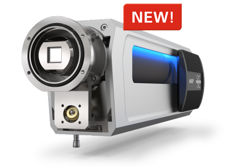
eWARP, the revolutionary EBSD detector, combines direct electron detection and CMOS technologies to maximize productivity and data quality. Image Credit: Bruker Nano Analytics
A Novel EBSD Detector Powered by Bruker’s Wide ARea Pixelated (WARP) Sensor Technology
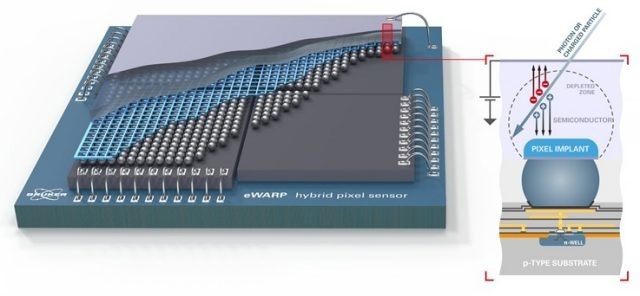
Schematic representation of Bruker’s hybrid pixel sensor technology, a.k.a. Wide Area Pixelated (WARP) sensor. Image Credit: Bruker Nano Analytics
At the heart of eWARP is the first-ever CMOS device featuring Bruker's patented on-chip binning technology. In binned mode, the sensor can capture up to 350,000 patterns per second, an extraordinary speed that enables the simultaneous acquisition of five ForeScatter Electron (FSE) images, each offering different blends of orientation and topographic contrast.
Beyond its immediate capabilities, eWARP’s unique binning technology opens the door to exciting opportunities for future advancements in microstructural analysis.
Signal Efficiency and Speed Gains Brought by eWARP
Ultra-High Resolution EBSD of an Additive Manufactured Steel, measured with eWARP
See in this video how EBSD mapping using the revolutionary new eWARP detector allows features that are just 100 nm wide to be resolved. Video Credit: Bruker Nano Analytics
eWARP’s gains in signal efficiency and speed mark a major advancement for the EBSD community. Here are a few key applications that will significantly benefit from eWARP’s performance:
- 3D EBSD: Faster, automated acquisition of data cubes using a plasma FIB-SEM, enabling either higher pixel resolution or the analysis of larger volumes.
- Beam-sensitive materials: With eWARP EBSD mapping is possible at very low electron doses, preserving delicate structures.
- Enhanced spatial resolution: Mapping of the finest features in ultra-fine-grained materials can be performed by operating at reduced accelerating voltages and probe currents, without sacrificing speed.
- Excellent data integrity on insulating materials: Improved beam stability delivers stable, reliable data.
- Improved data quality on martensitic or heavily deformed metals and alloys: Reduced interaction volume at lower accelerating voltages (e.g., 10 kV) enhances pattern quality.
- Time-resolved mapping: Rapid acquisition of repetitive maps and images every couple of seconds means that microstructural changes during in-situ heating or mechanical testing experiments can be tracked.
- Large-area mapping: Efficient analysis of larger samples and/or higher pixel resolution scans.